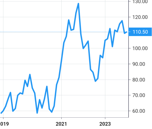
 Stock Value
About ASE Technology Holding
ASE Technology Holding Co., Ltd. and its subsidiaries (ASEH) provide a comprehensive range of semiconductors packaging, testing, and electronic manufacturing services (EMS).
ASEH directly controls ASE Group, SPIL Group, USI Group, and ASE Social Enterprise Co., Ltd.
USI Group engages primarily in EMS in relation to computing, consumer electronics, communications, industrial and automotive, among other services and businesses.
ASEH is a leading provider of semiconductor manufacturing services in assembly and testing. The company’s services include semiconductor packaging, production of interconnect materials, front-end engineering testing, wafer probing, and final testing services, as well as integrated solutions for EMS in relation to computing, peripherals, communications, industrial, automotive, and server applications.
The company is involved in all stages of the semiconductor manufacturing process except circuit design and wafer fabrication.
Strategy
The principal elements of the company’s strategy are to grow its packaging services and expand the company’s range of offerings; strategically expand and streamline production capacity; continue to leverage its presence in key centers of semiconductor and electronics manufacturing; and strengthen and develop strategic relationships with the company’s customers and providers of complementary semiconductor manufacturing services.
Principal Products and Services
The company offers a broad range of semiconductor packaging and testing services. In addition, the company provides EMS through USI Group. The company’s package types generally employ either leadframes or substrates as interconnect materials. The semiconductors the company packages are used in a wide range of end-use applications, including communications, computing, consumer electronics, industrial, automotive, and other applications. The company’s testing services include front-end engineering testing, which is performed during and following the initial circuit design stage of the semiconductor manufacturing process, wafer probe, final testing, and other related semiconductor testing services. The company focuses on packaging and testing semiconductors.
The company offers its customers turnkey services, which consist of packaging, testing, and direct shipment of semiconductors to end users designated by the company’s customers. The company’s EMS are used in a wide range of end-use applications, including, but not limited to, computing, peripherals, communications, industrial applications, automotive electronics, and server applications.
Packaging Services
The company offers a broad range of package types to meet the requirements of the company’s customers, including flip chip BGA, flip chip CSP, aCSP (advanced chip scale packages), quad flat packages (QFP), low profile and thin quad flat packages (LQFP/TQFP), bump chip carrier (BCC), quad flat no-lead (QFN) packages, aQFN (advanced QFN), and Plastic BGA. In addition, the company provides 3D chip packages, such as aMAP POP (advanced, laser ablation type), which enable the company’s customers to mount packages more easily, and HB PoP (High-Band package on Package) for higher performance orientation and marketing requirement.
The company also offers other forms of stacked die solutions in different package types, such as stacked die QFN, hybrid BGAs containing stacked wire bond, and FC die. Meanwhile, the company is developing cost-effective solutions to 3D packages, such as FOCOS (Fan-out Chip-on-Substrate) and 2.5D (silicon interposer), to fulfill current low-cost and high-performance requirements in parallel with 3D IC with TSV (Through Silicon Via) technology. In addition, to meet current trends toward low-cost solutions, the company provides copper wire bonding solutions, which can be applied to traditional gold wire products. The company also provides a high-volume manufacturing experience with silver wire bonding for FCCSP Hybrid packages. Furthermore, the company is one of the key providers of IoT (Internet of Things), server and automotive services. The company is among the leaders in such packaging processes and technologies and is well positioned to lead the technology migration in the semiconductor packaging industry.
To address the new demands of 5G wireless technology, the company surveys new materials and structures based on developed package structures and focuses the company’s efforts on developing more integration solutions, such as Application Processor (AP) module and RF front end (RFFE) with customized SiP services.
Wirebonding
The company provides wirebonding, including leadframe-based packages and substrate-based packages. Leadframe-based packages are packaged by connecting the die, using wire bonders, to the leadframe with gold wire or copper wire. As packaging technology improves, the number of leads per package increases. In addition, improvements in leadframe-based packages have reduced the footprint of the package on the circuit board and improved the electrical performance of the package. To have higher interconnected density and better electrical performance, semiconductor packages have evolved from leadframe-based packages to substrate-based packages. The company’s expertise in BGA packages also includes capabilities in stacked-die BGA, which assembles multiple dies into a single package.
The company has advanced PoP by the invention of aMAPPoP, which provides the package interconnects by exposing a molded in solder ball with a laser via. Aside from being cost-effective due to block molding, this PoP also has much lower warpage, greatly improving the stacking yield.
Advanced Packages
The company has focused on developing its capabilities in certain packaging solutions, such as aCSP (wafer-level chip scale package), flip chip BGA, Heat-Spreader FCBGA, flip-chip CSP, Hybrid FCCSP (Flip Chip + W/B), Flip Chip PiP (Package in Package), Flip Chip PoP (Package on Package), aS3TM (Advanced Single Sided Substrate), HB POP (High-Bandwidth POP), Fan-Out Wafer-Level Packaging, SESUB, and 2.5D. Flip-chip BGA technology replaces wire bonding with wafer bumping for interconnections within the package. Wafer bumping involves the placing of tiny solder balls, instead of wires, on top of dies for connection to substrates. As compared with more traditional packages, which allow input/output connection only on the boundaries of the dies, flip chip or wafer-level package solutions significantly enhance the input/output flow by allowing input/output connections over the entire surface of the dies.
Advance Embedded Assembly Substrate Integration (aEASI) is a technology, which allows the embedding of thin chips into substrate build-up layers. aEASI can be used in various technologies tailored to clients’ demands, such as package solution of miniaturization, and has also been proven to have better electrical/thermal performance. It also provides flexibility in design (such as for MicroSiP), and the electrical contacts to the chips are realized by laser-drilled and metallized micro-vias to replace the traditional wire bonding process. aEASI is mainly used in power management applications.
Wafer-Level MEMs (WL MEMs) is an advanced assembly technology for MEMs in wafer-level types instead of current LGA or leadframe types using TSV or chip-to-wafer technology. WL MEMs are mainly used in applications such as pressure, temperature, humidity, and gyroscope sensors, among others.
Fan-Out Wafer-Level Packages (FOWLP) provide an extended solution and package type to integrate different functional chips or packages, a reduction in resistance and inductance over FCCSP, better thermal performance, and smaller form factors of packages. FOWLP can be applied for different stack and SiP solutions.
The company provides numerous technologies to meet various customer demands.
Heterogeneous Integration
Heterogeneous Integration refers to the integration of separately manufactured components into a higher-level assembly that, in the aggregate, provides enhanced functionality and improved operating characteristics:
SiP and Modules
ASEH is a market leader in SiP technologies from design to assembly and high-volume manufacturing. SiP involves the integration of multiple components from IC chips and components, including ASICs, Memory, Analog & mixed signals devices, passives, MEMs, sensors, antennas, and other devices into one single package. SiP and Modules products are gaining significant traction within the industry, given growing demand for miniaturized electronic devices that deliver more functions and higher performance, lower power, greater speed, and increased bandwidth. ASEH’s SiP portfolio includes flip chip and wirebond multichip packaging, embedding technologies, such as SESUB and aEASI, and wafer-level technologies, including fan-out and IPD. IPD uses a wafer-level process to integrate passive components on an individual substrate. In addition, the company leverages some of its SMT-based technologies, such as compartment shielding, double-sided module, and antenna integration.
The company also offers module assembly services, which combine one or more packaged semiconductors with other components in an integrated module to enable increased functionality for system-level assembly. End-use applications for modules include cellular phones and wireless LAN applications, Bluetooth applications, camera modules, automotive applications, toys, networking, storage, and power management.
Fan-Out
With the packaging done on singulated die formed into a reconstituted molded wafer or panel, fan-out packaging enables multi-die packages, through partitioning with different nodes and functionality. Fan-out can be done either chip first or chip last, with both options resulting in much higher-density interconnect and improved cost efficiency. Initially fan-out was used primarily for smaller, lower I/O count packages, until the company introduced a very high-density fan-out alternative to 2.5D Interposer packages, Fan-out Chip on Substrate (FOCoS), a hybrid fan-out/FCBGA package. Fan-out is used in high-volume applications for a wide variety of products, including PMICs, RF packages, Baseband processors, and high-end networking systems.
As 5G, AI, and high-performance computing continue to make inroads on a global basis, there is an increased demand for semiconductor devices that deliver enhanced performance, lower latency, increased bandwidth, and greater power efficiency. ASEH strives to meet this demand by innovating 2.5D and 3D technologies that is becoming more central within the semiconductor industry. The company has established itself as a leader in 2.5D technology through the company’s successful pioneering of 2.5D solutions that helped bring advanced ASIC and HBM products to the marketplace. In addition, ASEH is introducing high-density fan-out technology for multi-die solutions to achieve high bandwidth and high-performance across the market landscape, addressing demand from high density data centers to consumer and mobile spaces.
Automotive Electronics
The company assembles automotive electronic products based on its leading technology, good quality systems, and automation. The company provides a variety of products, such as leadframe base, substrate base, Flip Chip, and Wafer-Level packages. The company also provides robust package solutions to customers and end-users, including most types of industrial package solutions together with tailor-made solutions to meet customers’ and end-users’ requirements for automotive specifications.
The company collaborates with certain customers to develop and release copper wire for advanced wafer process (40nm for QFP and 40 nm for BGA) development that will fulfill criteria in AEC-Q100 and under development of the 28 nm wafer process with variety packaging structure. In addition, the company offers the FOWLP solution for radar products according to requests from some tier 1 customers.
Interconnect Materials
The company produces substrates for use in the company’s packaging operations.
Testing Services
The company provides a complete range of semiconductor testing services, including front-end engineering testing, wafer probing, final testing of logic/mixed-signal/RF/(2.5D/3D) packages and SiP/MEMS/Discrete modules, and other test-related services.
The company’s testing services employ technology and expertise, which are among the most sophisticated in the semiconductor industry. In addition to maintaining different types of testing equipment, which enables the company to test a variety of semiconductor functions, the company works with its customers to design effective testing solutions on multiple equipment platforms for particular semiconductors.
Front-End Engineering Testing
The company provides front-end engineering testing services, including customized software development, electrical design validation, and reliability and failure analysis.
Customized Software Development
Test engineers develop customized software to test the semiconductors using the company’s equipment. Customized software, developed on specific test platforms, is required to test the conformity of each particular semiconductor type to its unique functionality and specification.
Electrical Design Validation
A prototype of the designed semiconductor is subjected to electrical tests using advanced test equipment and customized software. These tests assess whether the prototype semiconductor complies with a variety of different operating specifications, including functionality, frequency, voltage, current, timing, and temperature range.
Reliability Analysis
Reliability analysis is designed to assess the long-term reliability of the semiconductor and its suitability of use for intended applications. Reliability testing can include ‘burn-in’ services, which electrically stress a device, usually at high temperature and voltage, for a period of time long enough to cause the failure of marginal devices.
Failure Analysis
In the event that the prototype semiconductor does not function to specifications during either the electrical design validation or reliability testing processes, it is typically subjected to failure analysis to determine the cause of the failure to perform as anticipated. As part of this analysis, the prototype semiconductor may be subjected to a variety of analyses of electrical testing.
Wafer Probing
Wafer probing is the step immediately before the packaging of semiconductors and involves visual inspection and electrical testing of the processed wafer for defects to ensure that it meets the company’s customers’ specifications. Wafer probing services require expertise and testing equipment similar to that used in final testing, and most of the company’s testers can also be used for wafer probing.
Logic/Mixed-signal/RF/(2.5D/3D) Module and SiP/Discrete Final Testing
The company conducts final tests of a wide variety of logic/mixed-signal/RF/(2.5D/3D) packages and SiP/MEMS/discrete modules, with the number of leads or bumps ranging from the single digits to over 30 thousand and operating frequencies of over 32 Gbps for digital semiconductors and mmWave for 5G semiconductors, which are at the high end of the range for the industry. The products the company tests include applications for wired, wireless, and mobile communications, automotive, home entertainment, IoT, personal computer, artificial intelligence, and high-performance computing applications, as well as a variety of consumer and application-specific integrated circuits for various specialized applications.
Other Test-Related Services
The company provides a broad range of additional test-related services, such as:
Electric Interface Board and Mechanical Test Tool Design: Process of designing individualized testing apparatuses such as test load boards, sockets, handler change kits, and probe cards for unique semiconductor devices and packages.
Program Conversion: Process of converting a program from one-test platform to different test platforms to reduce testing costs or optimize testing capacity.
Program Efficiency Improvement: Process of optimizing the program code or increasing site count of parallel tests to improve testing throughout.
Burn-In Testing: Burn-in testing is the process of electrically stressing a device, usually at high temperature and voltage, for a period of time to simulate the continuous use of the device to determine whether this use would cause the failure of marginal devices.
Module and SiP Testing: The company provides module and SiP testing through an integrated bench solution or automatic test equipment to the company’s customers with a complete solution with respect to fingerprint sensor module, camera module, 3D depth sensing module, wireless connectivity devices, global positioning system devices, personal navigation devices, digital video broadcasting devices, RF front end devices, and 5G AiPs.
Tape and Reel: Process, which involves transferring semiconductors from a tray or tube into a tape-like carrier for shipment to customers.
Drop Shipment Services: The company offers drop shipment services for shipment of semiconductors directly to end users designated by the company’s customers. Drop shipment services are provided mostly in conjunction with logic/mixed-signal/RF/3D IC/discrete testing. The company provides drop shipment services to a significant percentage of its testing customers. A substantial portion of the company’s customers at each of the company’s facilities have qualified these facilities for drop shipment services. The company’s ability to successfully execute its full range of services, including drop shipment services, is an important factor in maintaining existing customers, as well as attracting new customers.
EMS
The company provides integrated solutions for EMS in relation to computing, peripherals, communications, industrial, automotive, and server applications through USI Group. The key products and services the company offers to its customers include:
Computing: Motherboards for server and desktop PCs, peripherals, port replicators, network attached systems, and solid state drives.
Communications: Wi-Fi and SiP.
Consumer Products: Control boards for flat panel devices and SiP.
Automotive Electronics: Automotive EMS, car LED lighting, and regulators/rectifiers.
Industrial Products: Point-of-sale systems and smart handheld devices.
Others: Field replacement units and return material authorization.
Sales and Marketing
Sales and Marketing Presence
The company maintains sales and marketing offices in Taiwan, the U.S., Belgium, Singapore, the P.R.C., Korea, Malaysia, Japan, and a number of other countries. The company also has sales representatives operating in certain other countries in which the company does not have offices. The company’s sales and marketing offices in Taiwan are located in Hsinchu, Taichung and Kaohsiung. The company conducts marketing research through its customer service personnel and through its relationships with its customers and suppliers the company endeavors to keep abreast of market trends and developments. The company also provides advice on production process technology to its major customers planning the introduction of new products.
Customers
The company packages and tests for its customers a wide range of products with end-use applications in the communications, computing, and consumer electronics/industrial/automotive sectors. The company’s EMS provide a wide range of products with end-use applications.
Intellectual Property
As of January 31, 2023, the company held 2,284 Taiwan patents, 1,914 U.S. patents, 1,858 P.R.C. patents, 13 Europe patents, and 30 patents in other countries related to various semiconductor packaging technologies and invention, utility, and design on the company’s EMS. In addition, as of January 31, 2023, the company had a total of 1,864 pending patent applications, 178 in Taiwan, 515 in the U.S., 1,153 in the P.R.C., 13 in Europe, and 5 in other countries. Moreover, the company filed several trademarks applications in Taiwan, the U.S., the P.R.C., and the EU. For example, ‘ASE,’ ‘aCSP,’ ‘a-EASI,’ ‘a-fcCSP,’ ‘aQFN,’ ‘a-QFN,’ ‘a-S3, ‘a-TiV,’ ‘aWLP,’ ‘a-WLP,’ ‘iSiP,’ ‘iWLP,’ ‘aSiM,’ ‘SiP-id’, ‘SPIL,’ ‘HSiP,’ ‘XnBay’, and ‘Emerald’ have been registered in Taiwan.
The company has also entered into various non-exclusive technology license agreements with other companies involved in the semiconductor manufacturing process, including Infineon Technologies AG, TDK Corporation, and DECA Technologies Inc. The technology the company licenses from these companies includes solder bumping, redistribution, ultra CSP assembly, advanced QFN assembly, wafer-level packaging, and other technologies used in the production of package types, such as BCC, flip chip BGA, film BGA, aQFN, and chip embedding. One of the company’s license agreements with Infineon Technologies AG will remain in effect until expiration of the patents licensed by the agreement, and the other automatically renews each year unless the parties to the agreement agree otherwise. The company’s license agreement with TDK Corporation will remain in effect until expiration of the TDK’s patents licensed by the agreement. The company’s license agreement with DECA will expire on January 13, 2026.
Research and Development
The company’s research and development expenses were NT$24,369.9 million (U.S.$793.0 million) in 2022.
Seasonality
The company’s first quarter (year ended December 2022) operating revenues have historically decreased over the preceding fourth quarter, primarily due to the combined effects of holidays in the U.S., Taiwan, and elsewhere in Asia.
Competition
The company’s EMS business faces significant competition from other EMS providers, such as Hon Hai Precision Industry Co., Ltd.
History
ASE Technology Holding Co., Ltd. was founded in 1984. The company was incorporated in 2018.