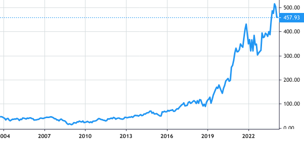
 Stock Value
About KLA Corp
KLA Corporation and its majority-owned subsidiaries (KLA) operate as a supplier of industry-leading equipment and services that enables innovation throughout the electronics industry.
The company provides advanced process control and process-enabling solutions for manufacturing wafers, reticles/masks, chemicals/materials, integrated circuits (‘IC’ or ‘chip’), packaged ICs, printed circuit boards (‘PCB’) and flat panel displays (‘FPD’), as well as comprehensive support and services across the company’s installed base. The company’s suite of advanced products, coupled with its unique yield management software and services, allow the company to deliver the solutions its customers need to achieve their productivity goals by significantly improving yields, reducing waste, reducing risks and reducing costs. This improves their overall profitability and return on investment.
Segments
The company operates through three reportable segments: Semiconductor Process Control; Specialty Semiconductor Process; and PCB, Display and Component Inspection.
Within the Semiconductor Process Control segment, the company’s comprehensive portfolio of inspection, metrology and software products, as well as related services, help IC, wafer, reticle/mask and chemical/materials manufacturers achieve target yields throughout the entire fabrication process, from R&D to final volume production. These products and services are designed to provide comprehensive solutions to help customers accelerate development and production ramp cycles, achieve higher and more stable product yields and improve their overall profitability.
Within the Specialty Semiconductor Process segment, the company develops and sells advanced vacuum deposition and etch process tools, which are used by a broad range of specialty semiconductor customers, including manufacturers of microelectromechanical systems (‘MEMS’), radio frequency (‘RF’) communication semiconductors, and power semiconductors for automotive and industrial applications.
Within the PCB, Display and Component Inspection segment, the company sells products and services that enable electronic device manufacturers to inspect, test and measure PCBs, IC substrates, FPDs and packaged ICs to verify their quality, pattern the desired electronic circuitry on the relevant substrate and perform three-dimensional shaping of metalized circuits on multiple surfaces.
Customers
The company counts among its largest customers the leading semiconductor, semiconductor-related and electronic device manufacturers in Asia, the U.S. and Europe.
For the year ended June 30, 2023, the company’s customers accounted for more than 10% of total revenues, primarily in the Semiconductor Process Control segment, were Taiwan Semiconductor Manufacturing Company Limited and Samsung Electronics Co., Ltd.
Sales, Service and Marketing
The company’s sales, service and marketing efforts aim to build deep long-term relationships with the company’s customers. The company focuses on providing comprehensive resources for the full breadth of process control, process-enabling and yield management solutions for manufacturing and testing wafers and reticles, a wide variety of ICs, PCBs, IC substrates, packaging, and flat and flexible panel displays, as well as general materials research. The company’s revenues are derived primarily from product sales and related service contracts, mostly through the company’s direct sales force.
The company has direct sales forces in Asia, the U.S. and Europe. The company maintains an export compliance program designed to meet the requirements of Commerce and the U.S. Department of State and the trade regulations of the international jurisdictions in which the company operates.
In addition to sales and service offices in the U.S., the company conducts sales, marketing and services out of subsidiaries or branches in many regions; some of the largest include China, Germany, Israel, Japan, Korea, Singapore, Taiwan and the United Kingdom.
Products and Services
KLA develops industry-leading process control and yield management solutions and services that enable innovation throughout the semiconductor and related electronics industries. The company provides advanced process control and process-enabling solutions for manufacturing wafers, reticles, ICs, packaging, PCBs, IC substrates and flat and flexible panel displays.
The Semiconductor Process Control segment offers a comprehensive portfolio of inspection, metrology, chemistry process control and software products and related services, which support the semiconductor ecosystem from R&D to final volume production. For IC manufacturing, the company’s systems support the production of all chip types, including advanced logic, DRAM, 3D NAND, power devices, MEMS, legacy design node chips and more. The company’s substrate manufacturing systems support the production of a broad range of wafer types and sizes, including silicon, prime silicon SOI, sapphire, glass, wide bandgap substrates (e.g., SiC and GaN) and more. The company’s reticle systems support quality control during the manufacturing of optical and EUV reticle types.
The company also produces products that support chemical/materials quality control, and process tool development and qualification. The company’s products and services for chip, wafer, reticle, packaging, solar, hard disk drive, original equipment manufacturer (‘OEM’) and chemical/materials manufacturing are designed to provide comprehensive solutions that help the company’s customers accelerate development and production ramp cycles, achieve higher and more stable product yields and improve their overall profitability. The Semiconductor Process Control segment offers a variety of solutions and products, including:
Chip Manufacturing: Defect Inspection and Review: Inspection and review tools are used to identify, locate, characterize, review, and analyze defects on various surfaces of patterned and unpatterned wafers. Products include 39xx Series, 29xx Series, C20x Series, eSL10, Voyager Series, 8 Series, Puma Series, CIRCL Series, Surfscan Series, Surfscan SP Ax Series, eDR7xxx Series.
Chip Manufacturing: Metrology: Metrology systems are used to measure pattern dimensions, film thickness(es), film stress, layer-to-layer alignment, pattern placement, surface topography and electro-optical properties for wafers. Products include Archer Series, ATL Series, Axion Series, SpectraShape Series, SpectraFilm Series, Aleris Series, PWG Series, Therma-Probe Series, OmniMap RS-xxx Series, MicroSense product family, CAPRES product family.
Wafer Manufacturing: Defect Inspection and Review, and Metrology: Wafer defect inspection, review and metrology systems are used to help wafer/substrate manufacturers manage quality throughout the wafer fabrication process by detecting defects, characterizing surface quality and assessing wafer geometry. Products include Surfscan Series, Surfscan SP Ax Series, eDR7xxx Series, WaferSight Series, Candela Series, MicroSense wafer geometry product family.
Reticle Manufacturing: Defect Inspection, Metrology and In Situ Process Management: Reticle inspection and metrology systems help reticle blank, patterned optical reticle, patterned EUV reticle, and chip manufacturers identify defects, pattern placement errors, and process issues during reticle manufacturing. In addition to reducing yield risk during production, these systems also support outgoing and incoming reticle quality control. Products include Teron SL6xx Series, Teron 6xx Series, TeraScan 5xx Series, X5.x Series, FlashScan Series, LMS IPRO Series, Microsense wafer geometry product family.
Chip Manufacturing: Chemistry Process Control: Chemical process control equipment qualifies incoming supplies, manages tool inputs, adjusts chamber/bath conditions and monitors process waste. Products include QualiSurf Series, Quali-Line Quanta Series, Quali-Line Prima Series, QualiLab Elite Series.
Chip Manufacturing: In Situ Process Management: Wired and wireless sensor wafers and reticles provide comprehensive data used to visualize, diagnose and control process conditions in the equipment used to manufacture chips and reticles. Additional wafer diagnostic solutions help troubleshoot and monitor materials handling to help detect and predict mechanical behaviors that may cause wafer damage. Products include SensArray product family.
Packaging Manufacturing: Wafer Inspection and Metrology, Chemistry Process Control: Wafer inspection and metrology systems for advanced wafer-level packaging help packaging manufacturers detect, resolve and monitor excursions to provide greater control of quality for improved device performance. Chemistry process monitoring systems analyze and monitor wet chemicals used in wafer-level packaging (WLP), panel-level packaging (PLP), and IC substrates. Kronos Series, CIRCL-AP, irArcher Series, PWG5 with XT Option, QualiSurf Series, Quali-Fill Libra Series, QualiLab Elite Series, Quali-Dose.
Semiconductor Software Solutions: Software solutions centralize and analyze the data produced by inspection, metrology and process systems for chip, wafer, reticle and packaging manufacturing. These solutions provide run-time process control, defect excursion identification, process corrections and defect classification to accelerate yield learning rates and reduce production risk. Patterning simulation software allows researchers to evaluate advanced patterning technologies, such as EUV lithography and multiple patterning techniques. Products include Klarity product family, 5D Analyzer, OVALiS, Anchor product family, RDC, FabVision Series, ProDATA, PROLITH, I-PAT, SPOT.
KLA Pro Systems: Certified and Remanufactured Products: Inspection and metrology systems support manufacture of larger design node chips and =200mm wafer manufacturing. Products include Surfscan Series, 2835, 2367, ASET-F5x Pro, Archer Series.
General Purpose/Lab Application: Specialty Semiconductor Manufacturing, Benchtop Metrology, Surface Characterization, Material Strength Characterization and Electrical Property Measurement. Products include Candela Series, HRP -260, Zeta Series, Tencor P Series, Nano Indenter Series, Alpha-Step Series, Filmetrics F Series, Filmetrics R Series, iMicro, iNano, Filmetrics Profilm3D Series, T150 UTM, NanoFlip, InSEM HT.
The Specialty Semiconductor Process segment develops and sells advanced vacuum deposition and etching process tools, which are used by a broad range of specialty semiconductor customers, including manufacturers of MEMS, RF communication chips and power semiconductors for automotive and industrial applications. The Specialty Semiconductor Process segment offers a variety of solutions and products, including:
Specialty Semiconductor Manufacturing: Etch, plasma dicing, deposition and other wafer processing technologies and solutions for the semiconductor and microelectronics industry. Products include SPTS Omega Series, SPTS Sigma Series, SPTS Delta Series, Primaxx Series, Xactix Series, SPTS Mosaic Series, MVD Series.
The PCB, Display and Component Inspection segment enables electronic device manufacturers to inspect, test and measure PCBs, IC substrates, FPDs and packaged ICs to verify their quality, pattern the desired electronic circuitry on the relevant substrate and perform three-dimensional shaping of metalized circuits on multiple surfaces. The PCB, Display and Component Inspection segment offers a variety of solutions and products, including:
PCB: Direct imaging, inspection, optical shaping, inkjet and additive printing, UV laser drilling, as well as computer-aided manufacturing and engineering solutions for the PCB and IC substrate market. Products include Orbotech Corus Series, Orbotech Infinitum Series, Orbotech Nuvogo Fine/ Nuvogo Series, Orbotech Diamond Series, Orbotech Ultra Dimension Series, Orbotech Ultra Fusion/ Fusion Series, Orbotech Discovery II Series, Orbotech Precise Series, Orbotech Ultra PerFix/ PerFix Series, Orbotech Neos Series, Orbotech Sprint Series, Orbotech Magna Series, Orbotech Jetext Series, Orbotech Apeiron Series, Frontline product family.
Display: Inspection and electrical testing systems to identify and classify defects, as well as systems to repair defects for the display market. Products include Orbotech Sirius Series, Orbotech Quantum Series, Orbotech Flare Series, Orbotech Array Checker Series, Orbotech Ignite Series, Orbotech Prism Series, Orbotech OASIS.
Component: Inspection and metrology systems for quality control and yield improvement in advanced and traditional semiconductor packaging markets. Products include ICOS F26x, ICOS Tx Series, Zeta-5xx/6xx.
Services
The company’s service programs enable its customers in all business sectors to maintain the high performance and productivity of the company’s products through a flexible array of service options. Whether a manufacturing site is producing wafers, reticles, ICs, display or PCB products, the company’s highly trained service teams collaborate with customers to determine the best products and services to meet technology and business requirements.
Competition
In each of the company’s product markets, the company has many competitors, including companies, such as Applied Materials, Inc., ASML Holding N.V., Hitachi High-Technologies Corporation, Onto Innovation, Inc. and Lasertec, Inc.
History
The company was founded in 1975. It was incorporated in 1975. The company was formerly known as KLA-Tencor Corporation and changed its name to KLA Corporation in 2019.

