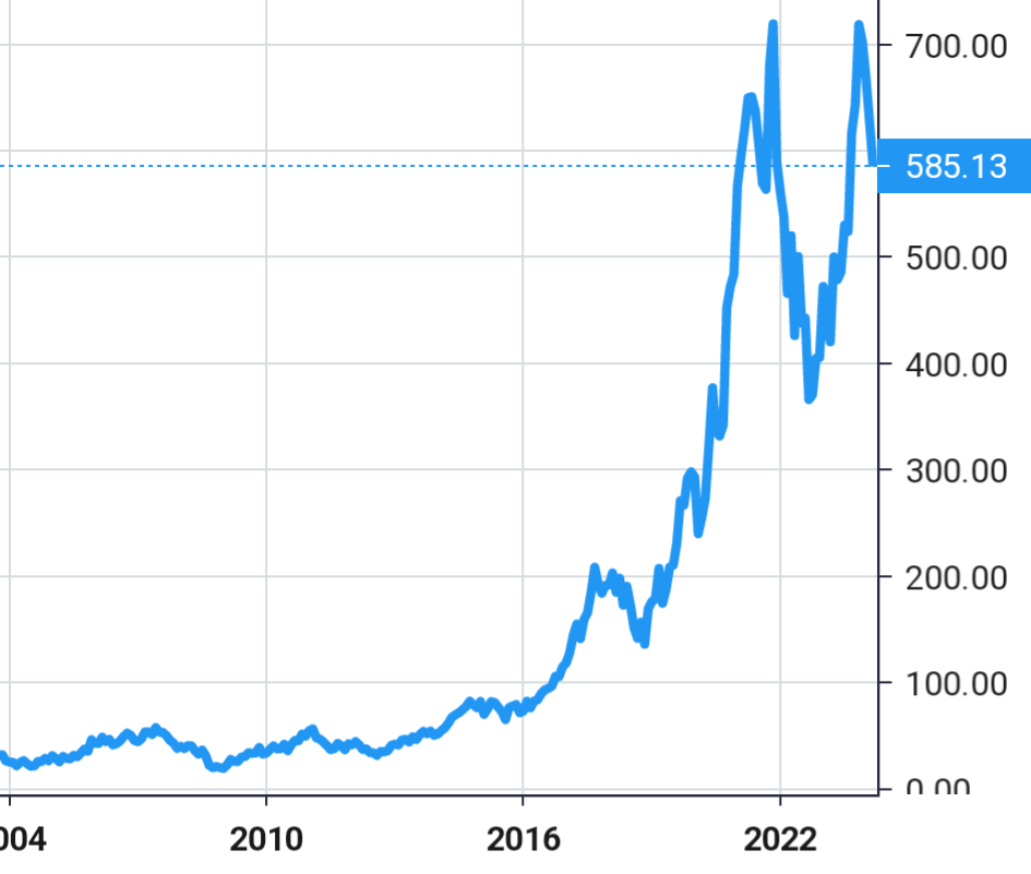
 Stock Value
About Lam Research
Lam Research Corporation (Lam) designs, manufactures, markets, refurbishes, and services semiconductor processing equipment used in the fabrication of integrated circuits.
The company maintains a network of facilities throughout Asia, Europe, and the United States in order to meet the needs of its dynamic customer base.
The company is a global supplier of innovative wafer fabrication equipment and services to the semiconductor industry. It has built a strong global presence with core competencies in areas, such as nanoscale applications enablement, chemistry, plasma and fluidics, advanced systems engineering, and a broad range of operational disciplines. The company’s products and services are designed to help its customers build smaller and better performing devices that are used in a variety of electronic products, including mobile phones, personal computers, servers, wearables, automotive vehicles, and data storage devices.
The company’s customer base includes leading semiconductor memory, foundry, and integrated device manufacturers (IDMs) that make products, such as non-volatile memory (NVM), dynamic random-access memory (DRAM), and logic devices. Their continued success is part of the company’s commitment to driving semiconductor breakthroughs that define the next generation. The company’s core technical competency is integrating hardware, process, materials, software, and process control enabling results on the wafer.
The company also addresses processes for back-end wafer-level packaging (WLP), which is an alternative to traditional wire bonding and can offer a smaller form factor, increased interconnect speed and bandwidth, and lower power consumption, among other benefits. The company offers advanced packaging solutions that support fan-out panel-level packaging, a process in which chips or chiplets are cut from a large format substrate sheet several times the size of a traditional silicon wafer, which increases yield and reduces waste and solutions that meet the need for 3D stacking of high bandwidth memory (HBM). In addition, the company’s products are well-suited for related markets that rely on semiconductor processes and require production-proven manufacturing capability, such as complementary metal-oxide-semiconductor image sensors (CIS) and micro-electromechanical systems (MEMS).
The company’s Customer Support Business Group (CSBG) provides products and services to maximize installed equipment performance, predictability, and operational efficiency. It offers a broad range of services to deliver value throughout the lifecycle of its equipment, including customer service, spares, upgrades, and new and refurbished non-leading edge products in its deposition, etch, and clean markets. Many of the technical advances that the company introduces in its newest products are also available as upgrades, which provide customers with a strategy for extending the performance and capabilities of their existing wafer fabrication lines. Service offerings include addressing productivity needs for its customers, including but not limited to, system uptime or availability optimization, throughput improvements, and defect reduction. Additionally, within CSBG, the company’s Reliant product line offers new and refurbished non-leading edge products in deposition, etch and clean markets for those applications that do not require the most advanced wafer processing capability.
Products
Deposition Processes and Product Families
Deposition processes create layers of dielectric (insulating) and metal (conducting) materials used to build a semiconductor device. Depending on the type of material and structure being made, different techniques are employed. Electrochemical deposition creates the copper wiring (interconnect) that links devices in an integrated circuit (IC or chip). Plating of copper and other metals is also used for Through-silicon Via (TSV) and WLP applications. Tiny tungsten connectors and thin barriers are made with the precision of chemical vapor deposition and atomic layer deposition, which adds only a few layers of atoms at a time. Plasma-enhanced chemical vapor deposition (CVD), high-density plasma CVD, and atomic layer deposition (ALD) are used to form the critical insulating layers that isolate and protect all of these electrical structures. Lastly, post-deposition treatments, such as ultraviolet thermal processing are used to improve dielectric film properties.
ALTUS Product Family
Tungsten and/or Molybdenum deposition is used to form conductive features, such as contacts, vias, and wordlines on a chip. These features are small, often narrow, and use only a small amount of metal, so minimizing resistance and achieving complete fill can be difficult. At these nanoscale dimensions, even slight imperfections can impact device performance or cause a chip to fail. The company’s ALTUS systems combine CVD and ALD technologies to deposit the highly conformal or selective films as needed for advanced tungsten metallization applications in both logic and memory. The Multi-Station Sequential Deposition architecture enables nucleation layer formation and bulk CVD/ALD fill to be performed in the same chamber (in situ). The company’s ALD technologies are used in the deposition of barrier films to achieve high step coverage with reduced thickness at lower temperatures relative to a conventional process.
SABRE Product Family
Copper deposition lays down the electrical wiring for most semiconductor devices. Even the smallest defect - say, a microscopic pinhole or dust particle - in these conductive structures can impact device performance, from loss of speed to complete failure. The SABRE ECD (electrochemical deposition) product family, which helped pioneer the copper interconnect transition, offers the precision needed for copper damascene manufacturing in logic and memory. System capabilities include cobalt deposition for logic applications and copper deposition directly on various liner materials, which is important for next-generation metallization schemes. For advanced WLP applications, such as forming conductive bumps, redistribution layers, TSV filing, and wafer level bonding, the SABRE 3D family combines Lam’s SABRE Electrofill technology with additional innovation to deliver the high-quality films needed at high productivity. The modular architecture can be configured with multiple plating and pre/post-treatment cells, providing flexibility to address a variety of packaging applications, including HBM.
SPEED Product Family
Dielectric gapfill processes deposit critical insulation layers between conductive and/or active areas by filling openings of various aspect ratios between conducting lines and between devices. With advanced devices, the structures being filled can be very tall and narrow. As a result, high-quality dielectric films are especially important due to the ever-increasing possibility of cross-talk and device failure. The company’s SPEED Gapfill High-Density Plasma CVD (HDP-CVD) products provide a multiple dielectric film solution for high-quality gapfill with industry-leading throughput and reliability. SPEED products have excellent particle performance, and their design allows large batch sizes between cleans and faster cleans.
Striker Product Family
The latest memory, logic, and imaging devices require extremely thin, highly conformal dielectric films for continued device performance improvement and scaling. For example, ALD films are critical for spacer-based multiple patterning schemes where the spacers help define critical dimensions, as well as for insulating liners and gapfill in high aspect ratio features, which have little tolerance for voids and even the smallest defect. The Striker single-wafer ALD products provide dielectric film solutions for these challenging requirements through application-specific material, process and hardware options that deliver film technology and defect performance.
VECTOR Product Family
Dielectric film deposition processes are used to form some of the most difficult-to-produce insulating layers in a semiconductor device, including those used in the latest transistors and 3D structures. In some applications, these films require dielectric films to be exceptionally smooth and defect free since slight imperfections are multiplied greatly in subsequent layers. The company’s VECTOR Plasma-enhanced CVD (PECVD) products are designed to provide the performance and flexibility needed to create these enabling structures within a wide range of challenging device applications. As a result of its design, VECTOR produces superior thin film quality, along with exceptional within-wafer and wafer-to-wafer uniformity.
Etch Processes and Product Families
Etch processes help create chip features by selectively removing dielectric (insulating), metal, silicon and poly silicon (conducting/semiconducting) materials that have been added during deposition. These processes involve fabricating increasingly small, complex, and narrow features using many types of materials. The primary technology, reactive ion etch, bombards the wafer surface with ions (charged particles) to remove material. For the smallest features, atomic-layer etching (ALE) removes a few atomic layers of material at a time. While conductor etch processes precisely shape critical electrical components like transistors, dielectric etch forms the insulating structures that protect conducting parts.
Flex Product Family
Dielectric etch carves patterns in insulating materials to create barriers between the electrically conductive parts of a semiconductor device. For advanced devices, these structures can be extremely tall and thin and involve complex, sensitive materials. Slight deviations from the target feature profile - even at the atomic level - can negatively affect electrical properties of the device. To precisely create these challenging structures, the company’s Flex product family offers differentiated technologies and application-focused capabilities for critical dielectric etch applications. Uniformity, repeatability, and tunability are enabled by a unique multi-frequency, small-volume, confined plasma design. Flex offers in situ multi-step etch and continuous plasma capability that delivers high productivity with low defectivity.
Vantex Product Family
Dielectric etch processes remove non-conductive materials during the manufacturing of a semiconductor device. Leading-edge memory devices have especially challenging structures, such as extremely deep holes and trenches, that must be manufactured with tight tolerances. The company’s latest dielectric etch system, Vantex creates high aspect ratio device features while maintaining critical dimension (CD) uniformity and selectivity. Vantex is part of the company’s Sense.i platform and offers advanced RF technology and repeatable wafer-to-wafer performance enabled by Equipment Intelligence to meet the needs of advanced memory manufacturing, primarily in 3D NAND high aspect ratio hole, trench, contact, and capacitor cell applications.
Kiyo Product Family
Conductor etch helps shape the electrically active materials used in the parts of a semiconductor device. Even a slight variation in these miniature structures can degrade device performance. In fact, these structures are so tiny and sensitive that etch processes push the boundaries of the basic laws of physics and chemistry. The company’s Kiyo product family delivers the high-performance capabilities needed to precisely and consistently form these features precisely and with high productivity. Proprietary Hydra technology in Kiyo products improves CD uniformity by correcting for incoming pattern variability, and atomic-scale variability control with production-worthy throughput is achieved with plasma-enhanced ALE capability.
Syndion Product Family
Plasma etch processes used to remove single crystal silicon and other materials deep into the wafer are collectively referred to as deep silicon etch. These may be deep trenches for CMOS image sensors, trenches for power and other devices, TSVs for HBM and advanced packaging, and other high aspect ratio features. These are created by etching through multiple materials sequentially, where each new material involves a change in the etch process. The Syndion etch product family is optimized for deep silicon etch, providing the fast process switching with depth and cross-wafer uniformity control required to achieve precision etch results. The systems support both conventional single-step etch and rapidly alternating process, which minimizes damage and delivers precise depth uniformity.
Versys Metal Product Family
Metal etch processes play a key role in connecting the individual components that form an IC, such as forming wires and electrical connections. These processes can also be used to drill through metal hardmasks that are used to form the wiring for advanced devices. To enable these critical etch steps, the Versys Metal product family provides high-productivity capability on a flexible platform. Superior critical dimension (CD), profile uniformity, and uniformity control are enabled by a symmetrical chamber design with independent process tuning features.
Clean Processes and Product Families
Clean techniques are used between manufacturing steps to clear away particles, contaminants, residues and other unwanted material that could later lead to defects and to prepare the wafer surface for subsequent processing. Wet processing technologies can be used for wafer cleaning and etch applications. Plasma bevel cleaning is used to enhance die yield by removing unwanted materials from the wafer’s edge that could impact the device area.
Coronus Product Family
Bevel cleaning removes unwanted masks, residues, and films from the edge of a wafer between manufacturing steps. If not cleaned, these materials become defect sources. For instance, they can flake off and re-deposit on the device area during subsequent processes. Even a single particle that lands on a critical part of a device can ruin the entire chip. By inserting bevel clean processes at strategic points, these potential defect sources can be eliminated and more functional chips produced. By combining the precise control and flexibility of plasma with technology that protects the active die area, the Coronus bevel clean family cleans the wafer’s edge to enhance die yield. The systems provide active die area protection by using plasma processing with proprietary confinement technology. Applications include post-etch, pre- and post-deposition, pre-lithography, and metal film removal to prevent arcing during plasma etch or deposition steps.
DV-Prime, Da Vinci, EOS, and SP Series Product Families
Wafer cleaning is performed repeatedly during semiconductor device manufacturing and is a critical process that affects product yield and reliability. Unwanted microscopic materials - some no bigger than the tiny structures themselves - need to be cleaned effectively. At the same time, these processes must selectively remove residues that are chemically similar to the device films. For advanced WLP, the wet clean steps used between processes that form the package and external wiring have surprisingly complex requirements. These processes are called on to completely remove specific materials and leave other fragile structures undisturbed. In IoT products that include power devices, MEMS and image sensors, there is a unique requirement for wafer backside wet etch to uniformly thin the silicon wafer while protecting the device side of the wafer.
Based on the company’s pioneering single-wafer spin technology, the DV-Prime and Da Vinci products provide the process flexibility needed with high productivity to address a wide range of wafer cleaning steps throughout the manufacturing process flow. As the latest of Lam’s wet clean products, EOS delivers exceptionally low on-wafer defectivity and high throughput to address progressively demanding wafer cleaning applications. With a broad range of process capability, the company’s SP Series products deliver production-proven wet clean and silicon wet etch solutions for challenging WLP and IoT applications.
Marketing, Sales, and Service
The company maintains ongoing service relationships with its customers and has an extensive network of service engineers in place throughout the United States, China, Europe, India, Japan, Korea, Southeast Asia, and Taiwan.
International Sales
A significant portion of the company’s sales and operations occur outside the United States.
Customers
The company’s customers include many of the world’s leading semiconductor manufacturers. The company’s most significant customers during the year ending June 25, 2023, included Intel Corporation; Kioxia Corporation; Micron Technology, Inc.; Samsung Electronics Company, Ltd.; and Taiwan Semiconductor Manufacturing Company.
Trademarks
The Lam Research logo and Lam Research are either registered trademarks or trademarks of the company or its subsidiaries in the United States and/or other countries.
Competition
The company’s primary competitor in the dielectric and metals deposition market is Applied Materials, Inc. For ALD and PECVD, the company also competes against ASM International and Wonik IPS. In the etch market, the company’s primary competitors are Applied Materials, Inc.; Hitachi, Ltd.; and Tokyo Electron, Ltd. Its primary competitors in the wet clean market are Screen Holding Co., Ltd.; Semes Co., Ltd.; and Tokyo Electron, Ltd.
History
Lam Research Corporation was founded in 1980. The company was incorporated in 1980.

